
Wafer thinning process for semiconductor wafers (GaAs wafers)
We have proven experience in the mass production of 30 µm thin wafers.
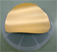 GaAs wafer processed up to 30 μm thickness |
Wafer Hard Support System
- Provides stable wafer thinning processing with hard support from sapphire substrates, etc.
- Thin metal film processing is also available with hard support.
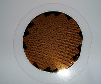 Product attached to hard support substrate |
Backside polishing process and removal of distortion layer after backside polishing
For wafer thinning processing of brittle materials such as GaAs, InP, etc., we provide BG, Polishing, and Etching processes to remove the distortion layer.