
Backside Processing
We provide an integrated service from wafer thinning, grinding and polishing to backside electrode attachment.
| Processing Performance | GaAs | 30μm~ available |
| InP | 80μm~ available | |
| Si | 30μm~ available |
- Back grinding of various types of wafers
- Backside metal attachment processing of various types of wafers
In recent years, devices for high-frequency applications have been required to have even greater capabilities. The challenge is to process the backside of the wafer, which involves making the wafer ever thinner. As such thin wafers are very difficult to handle, we have solved this issue by performing the entire operation from backside processing to dicing in one integrated process.
1.Backgrinding Processing Specifications
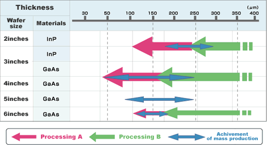
Two specifications of backgrinding processes are currently in mass production. As shown in the table below, the two backgrinding processes are divided into two categories: Process A, which is for thin backgrinding (100 to 150 µm or less), and Process B, which is for thicker backgrinding (100 to 150 µm or more).
Process A: Processing of thicknesses of 150 µm or less
Process using sapphire or other support substrates
Process B: Processing of thicknesses of 150 µm or more
Process using BG tape
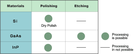
2.Backgrinding distortion removal method
A combination of polishing and etching is used to remove distortion.
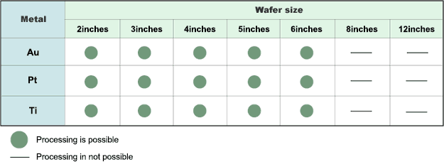
3.Backside metallization process
Sputtering equipment is used for backside metallization.
4.Gold plating process *Wafer in-plane thickness variation
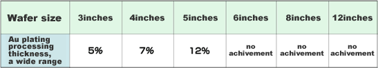
About Au plating. We adopt field plating taking the environment into consideration without using outside influences.