
Easy! What is a semiconductor?
1.About dicing process
What is dicing process?
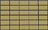
The wafer after dicing.(Enlarged view)
Dicing is cutting the wafer to pellets after a pretreatment process (pattern forming step in the semiconductor). Currently the most popular dicing equipment is the dicer. Dicing work consists of aligning the wafer position, X direction dicing, Y direction dicing, cleaning, and drying but recently it is done by full automation. Dicing is putting the groove in the scribe area of the fastened wafer by rotating the blade (which is a hardened diamond powder with a special metal) with very high-speed. It is important to clean with plenty of water while putting in the grooves.
Below, we show 2 kinds of dicing process specifications.
 The part of blade
- Half-cut dicing … Dicing method that cuts halfway through the wafer depth direction.
- Half-cut dicing … Dicing method that cuts halfway through the wafer depth direction.
We think that the dicing technology will make a lot of progress by the continuous appearance of new materials, improvement of processing quality and the requirement of microscopic high‐precision machining in the future.
2.Optical semiconductor
What is an optical semiconductor?
There are “semiconductors that light when they electrified” and “semiconductors that generate electricity when exposed to light” and we call them optical semiconductors.
The thing that changes electricity into light
“The semiconductor that lights when it is electrified” is called a light emitter such as a Laser and LED (Light Emitting Diode). Laser is used for reading and writing pictures or sound data by flashing on to disks such as a DVD or CD. Also laser has been used to send light information to optical fiber in optical communication. LED (Light Emitting Diode) is a glowing small part that is attached to electrical products. It has a low environmental load and the power consumption is 1/3 of an electric bulb and 2/3 of a fluorescent light. Recently it is used for traffic signals.
The thing that changes light into electricity
“The semiconductor that generates electricity when exposed to light” is called a light receiving element and typical products are called photodiodes. Photodiodes are also in use for reading and writing pictures or sound data to DVD’s or CD’s with laser. Also photodiodes have been used to receive light information from optical fiber in optical communication. A large number of optical semiconductors are invisible but used around us.
3.Diode
What is diode?
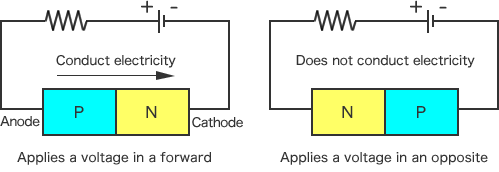
Diode is a semiconductor part that sends a current of electricity one-way. The element of the diode has a structure called a PN joint. Terminals from the P-type semiconductor are called Anode and terminals from N-type semiconductor are called Cathode. Diode sends only an electrical current that flows from the Anode to the Cathode and hardly conducts opposite flow of electricity. This effect is called a rectifying action and in other words, it’s the effect that converts alternating current to direct current.
Structure of the diode
The structure of diode is mostly a Si planar structure. Planar structure is used for MOS-LSI and has a stable performance and is strong to pollution. Diode is eventually used as packaged Si chips. There are mainly 2 types of packaging method, one is glass-sealing and the other is resin-sealing.
Glass-sealing is a sealed Si chip in a glass tube by melting the glass with heat after putting Si chip between lead wires attached to metal in the glass tube.
Resin mold is the mainstream for resin-sealing. It is the wiring of Au wire by wire bonding from Si chip surface after attaching Si chip to lead frame then hardened all together with resin.
Use of diode
- Used as a rectifier that converts alternating current to direct current in a power supply.
- Used to detect signals from high-frequency radio.
- Used as a switch to control ON and OFF power.
It is used in a very wide range of applications.
4.IC
What is IC?
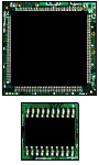
※The parts that contains IC
IC (integrated circuit) is like a 1cm square electrical part that has an electrical circuit inside.
An electrical circuit is a circuit that calculates and makes electrical signals bigger. We can watch TV or listen to music by a combination of both of them. It is used in every single thing that uses electricity such as a TV or a mobile phone.
IC is actually gold in appearance because it is covered with metals such as gold and copper but it normally is in a black plastic box which has legs on the side and under it.
5.About back grinding and polishing
About back grinding
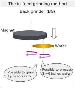
Back grind (BG) is one of the semiconductor manufacturing processes that make the wafer thickness uniform by grinding the back side of the wafer.
The back grinding practical method recently is called the in-feed system. This system grinds the wafer to predetermined thickness by grinding the adsorb wafer on the table called a rotating chuck with lowering grindstone which has set above gradually.
About back polishing
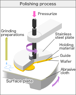
Polishing makes the wafer’s back side to a mirror surface while maintaining the dimensional accuracy. The polishing process is polishing the wafer with flowing grinding preparations with an abrasive cloth on the surface plate after holding the wafer to the plate with a holding material and guide.
The following points are essential to obtain quality while polishing.
- Wafer flatness
- No scratches, dirt, or pollution
- No processing strain
6.What is GaAs?
What is a compound semiconductor?
A compound semiconductor is a semiconductor material that is a combination of two kind of elements (Ⅴ group and Ⅲ group) and one is Ga (gallium) and the other is As (arsenic). The mainstream of the semiconductor is Si of the Ⅳ group but compound semiconductors convert electrical signals into light and radio waves and converts light and radio waves into electrical signals.
Merit of GaAs
It is said that IC’s using GaAs operate faster and the power consumption is reduced to about 1/3 and that it is easier to make smaller compared to IC’s using Si. However they are difficult to process because they are expensive and have a lot of crystal defects of the substrate so they are more fragile compared to Si. They are now popular mainly in the applications that require small but high performance such as mobile phones because GaAs devices came to be provided with low cost by advances in fine processing technology recently.
Nature of GaAs
- 【Physical properties】 Molecular formula: GaAs, Molecular weight: 144.64, Melting point: 1238℃ (1 atmospheric pressure), Density : solid 5.31(room temperature), It breaks down when it is heated to nearly 400℃ and it generates a highly toxic arsenic vapor.
- 【Chemical properties】 It hardly reacts with water but it reacts with steam, acid, and acid vapors and generates a harmful AsH3 (arsine).
Toxicity of GaAs
GaAs has been excluded from designation in the Poisonous and Deleterious Substances in the ”Poisonous and Deleterious Substances designation ordinance”. However, we need caution in handling it because it is designated as toxic substance in the laws below.
- Water Pollution Prevention Act
- Law of Waste Disposal and Cleaning
- Agricultural Land Soil Pollution Prevention Law